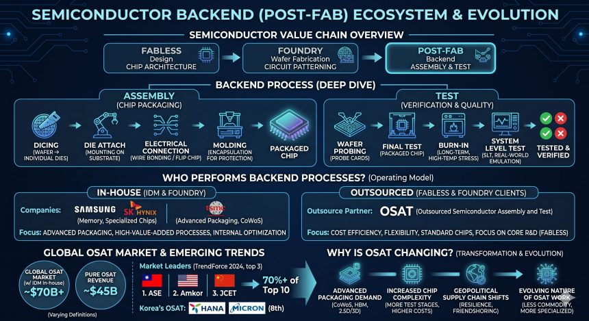
The semiconductor industry is undergoing a major transformation where success is no longer defined only by how small a chip can be built but by how efficiently it can be designed, packaged, and scaled for global use. From smartphones and EVs to AI servers and cloud systems, every modern technology relies on advanced chip integration that boosts performance while lowering power consumption.
At the centre of this ecosystem lies the PCB board, which forms the critical foundation connecting chips, memory, and power components into a complete system. Without a properly optimised PCB, even the most advanced semiconductor designs cannot deliver their full performance in real-world applications.
For readers, this topic is important because it shows how modern electronics actually move from concept to mass production. Whether you are an engineer, tech enthusiast, or someone curious about global supply chains, understanding the journey from design to OSAT (Outsourced Semiconductor Assembly and Test) gives a clear picture of how innovation scales into real-world technology.
The Evolution from Design to OSAT
Traditionally, semiconductor companies focused heavily on chip design, while manufacturing and testing were handled separately in different parts of the world. However, as chips have become more complex, this separation is no longer efficient. Today, the industry works in a tightly connected flow where design decisions directly influence packaging and production outcomes.
OSAT providers now play a much more strategic role than before. They are not just responsible for assembling and testing chips; they actively collaborate during early design stages to ensure that chips can be manufactured efficiently at scale.
This shift has created a more unified production ecosystem where performance, cost, and manufacturability are considered together rather than in isolation. As a result, companies can reduce failures, improve yield, and speed up time-to-market for advanced semiconductor products.
Why Advanced Packaging Is a Game Changer
Advanced packaging has become one of the biggest enablers of next-generation computing. Instead of relying only on transistor scaling, companies now combine multiple dies, layers, and functionalities into a single compact package.
This approach allows better performance without drastically increasing chip size or power consumption. It also helps solve major challenges related to heat management, signal delay, and system integration.
In simple terms, advanced packaging bridges the gap between raw silicon performance and real-world usability.
Role of PCB Board in System-Level Performance
The PCB board design process plays a crucial role in ensuring that advanced semiconductor systems function correctly once they are integrated into devices. A well-designed PCB ensures that signals move efficiently between components, power is distributed evenly, and thermal conditions remain stable.
As chip architectures become more advanced, PCB engineering must also evolve. High-speed signals, multi-layer routing, and advanced materials are now standard requirements in modern designs.
The importance of PCB design becomes even clearer when you look at system performance at scale. A weak PCB board layout can limit the performance of even the most powerful chips, creating bottlenecks that reduce efficiency and reliability.
This is why PCB engineering and semiconductor packaging must work closely together throughout the development cycle.
Scaling Challenges in Global Semiconductor Production
As semiconductor demand continues to rise globally, scaling production has become increasingly complex. It is no longer just about building chips; it is about building them consistently, efficiently, and across multiple regions with minimal variation.
One of the biggest challenges is maintaining consistency across design, fabrication, and testing stages. Even small variations in packaging or assembly can significantly affect performance at scale.
Another challenge is supply chain coordination. Modern chips rely on materials, equipment, and processes that span multiple countries, making synchronisation critical.
Key challenges in scaling semiconductor production:
- Increasing complexity of chiplet and multi-die architectures
- Thermal and power management limitations in dense packaging
- Global supply chain dependencies across fabrication and OSAT facilities
- Maintaining yield and quality consistency at high-volume production
These challenges are pushing companies to adopt more integrated workflows, where design, packaging, and testing are planned together from the beginning rather than treated as separate stages.
Integration Across the Semiconductor Ecosystem
Today’s semiconductor ecosystem is highly interconnected. The journey from initial chip design to final product delivery involves continuous feedback between multiple engineering teams.
The process typically moves through several key stages, starting with architecture design and simulation, followed by package planning, prototyping, OSAT assembly, and final system integration. Each stage influences the next, creating a loop of constant refinement and improvement.
This integrated model is especially important for US best semiconductor companies, which are heavily investing in advanced packaging technologies to maintain leadership in global markets. Their focus is not only on building powerful chips but also on ensuring that those chips can be manufactured and scaled efficiently for global demand.
The result is a more collaborative industry where design and manufacturing are no longer separate silos but parts of a continuous innovation pipeline.
Future of Advanced Packaging and Global Scaling
The future of semiconductor production will be shaped by tighter integration, smarter automation, and more modular architectures. Technologies like chiplets, 3D stacking, and heterogeneous integration are already redefining how systems are built.
We are also seeing increased use of AI-driven testing and simulation tools that help reduce errors before physical production begins. This improves yield and reduces costs, especially at large scale.
As these technologies evolve, the boundary between design, packaging, and system integration will continue to blur. Companies that can successfully unify these stages will have a significant advantage in delivering high-performance, cost-efficient products globally.
Conclusion
The journey from design to OSAT is the backbone of modern semiconductor innovation, ensuring advanced chips move smoothly from concept to mass production through a highly coordinated process. Every stage, from system-level optimisation to advanced packaging integration, plays a key role in overall product success while continuously improving performance and efficiency.
As demand grows across AI, automotive, and cloud computing, collaboration between design teams, OSAT providers, and ecosystem partners becomes even more critical. Ultimately, the ability to scale advanced packaging efficiently will define the next generation of global semiconductor leaders.
Tessolve is a semiconductor engineering company providing design, testing, and validation services to speed up chip development. At the core of advanced innovation, Tessolve bridges design and production for faster, reliable scaling. It serves industries like AI, automotive, and computing to deliver efficient, high-performance solutions.